Transitioning from a breadboard prototype to a custom Printed Circuit Board (PCB) marks a significant step for any new maker. While breadboards are invaluable for rapid prototyping and concept validation, they introduce limitations in terms of reliability, signal integrity, and physical size. Custom PCBs address these challenges directly, providing a robust, compact, and professionally finished platform for electronic circuits. Understanding the fundamental principles of PCB design is not merely a technical exercise; it is a critical skill that enables the creation of durable, repeatable, and scalable electronic projects, whether for personal use, educational purposes, or eventual commercial application. This guide outlines the essential concepts and workflow for new makers to confidently approach their first PCB design.
The Foundation: What is a PCB?
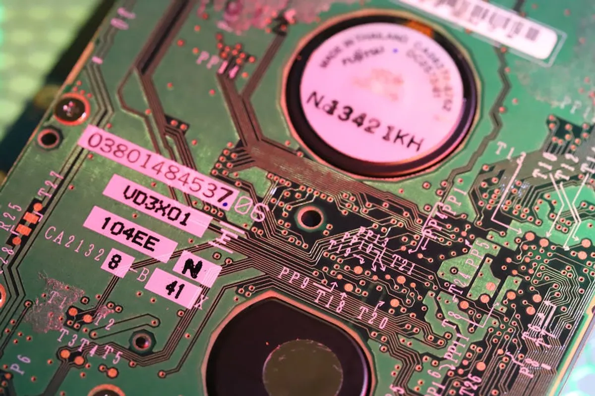
A Printed Circuit Board serves as the physical foundation for electronic components, providing mechanical support and electrical connections. It replaces the tangled wires of a breadboard with precisely etched conductive pathways, or traces, on a non-conductive substrate. PCBs are typically composed of multiple layers:
- Substrate: The insulating material, often fiberglass (FR-4), that forms the core of the board.
- Copper Layers: Thin sheets of copper laminated onto the substrate, etched to form traces, pads (for component attachment), and planes (for power or ground).
- Solder Mask: A protective layer, usually green, applied over the copper traces to prevent accidental short circuits during soldering and protect against environmental factors.
- Silkscreen: A white (or other color) ink layer printed on top of the solder mask, providing component designators, outlines, and other helpful markings for assembly and troubleshooting.
Key benefit: This layered structure allows for complex interconnections in a compact form factor, significantly reducing the physical size and increasing the reliability of electronic assemblies compared to point-to-point wiring.
Beyond the Breadboard: Why PCBs Matter
For new makers, the shift from breadboards to PCBs offers several compelling advantages:
- Reliability: Solder joints on a PCB are mechanically and electrically stable, unlike intermittent breadboard connections. This reduces debugging time and improves long-term project functionality.
- Compactness: Components can be placed much closer together, and traces routed efficiently, leading to significantly smaller and lighter designs. This is crucial for portable or space-constrained projects.
- Signal Integrity: Controlled trace impedance and reduced parasitic capacitance on a PCB minimize signal degradation, especially important for high-speed digital or sensitive analog circuits.
- Repeatability: Once designed, a PCB can be manufactured identically multiple times, ensuring consistent performance across all units. This is essential for batch production or sharing designs.
- Professional Appearance: A custom PCB lends a polished, professional look to any project, enhancing its perceived value and functionality.
The Design Workflow: From Concept to Copper
PCB design follows a structured workflow, typically involving schematic capture, layout, and preparation for manufacturing. Each phase builds upon the previous one, ensuring a logical and error-checked progression.
Schematic Capture: The Circuit's Blueprint
The first stage involves creating a schematic diagram, which is a logical representation of your electronic circuit. In a schematic, components are represented by abstract symbols (e.g., a resistor symbol, an op-amp symbol), and their interconnections are shown as lines, or nets. This stage focuses purely on the electrical functionality without considering physical placement or dimensions.
During schematic capture, you will:
- Select Components: Choose the specific integrated circuits, resistors, capacitors, and connectors required for your design. Each component will have an associated symbol and, crucially, a footprint (the physical pattern on the PCB for soldering).
- Draw Connections (Nets): Connect component pins logically to define current paths and signal flow. Each unique connection is assigned a net name.
- Assign Values and Properties: Specify resistor values, capacitor types, and other component parameters.
- Perform Electrical Rules Check (ERC): Most design software includes an ERC tool that identifies common electrical errors, such as unconnected pins or shorted power supplies, ensuring the schematic is electrically sound.
Commercial utility: A well-documented schematic is indispensable for debugging, future modifications, and collaboration with other engineers, serving as the definitive electrical reference for the project.
PCB Layout: Translating Logic to Physical Form
Once the schematic is complete and verified, the next step is PCB layout. This involves translating the logical connections from the schematic into physical copper traces on the board. This phase requires careful consideration of mechanical constraints, electrical performance, and manufacturing requirements.
Key layout tasks include:
- Board Outline Definition: Establishing the physical dimensions and shape of your PCB, often dictated by an enclosure or mounting requirements.
- Component Placement: Strategically positioning each component on the board. This is a critical step, influencing signal integrity, thermal management, and ease of assembly. Components should be grouped logically, with high-speed signals kept short and power components placed to facilitate heat dissipation.
- Routing Traces: Drawing the copper traces that connect component pads according to the nets defined in the schematic. This involves selecting appropriate trace widths, clearances, and deciding which layer each trace will occupy. Vias (plated holes) are used to transition traces between layers.
- Adding Planes: Dedicating entire copper layers or sections for ground and power planes. These planes provide stable power distribution, reduce electromagnetic interference (EMI), and improve thermal performance.
Design Rules Check (DRC): Ensuring Manufacturability
Before finalizing your layout, performing a Design Rules Check (DRC) is mandatory. This automated process verifies that your PCB layout adheres to a set of manufacturing constraints provided by your chosen PCB fabrication house. These rules dictate minimum trace width, minimum spacing between traces, pad-to-trace clearances, drill hole sizes, and more. Failing to pass DRC will likely result in manufacturing errors or increased costs.
Pro Tip: Always obtain the specific Design Rule Check (DRC) parameters from your chosen PCB fabrication service before starting your layout. Using generic rules can lead to boards that are either unmanufacturable or unnecessarily expensive. Verify component footprints against datasheets, as incorrect footprints are a common and costly error for new designers.
Preparing for Fabrication
After a successful DRC, your PCB design is ready to be sent to a manufacturer. This involves generating specific files that the fabrication house uses to produce your physical board.
Generating Manufacturing Files
The industry standard for PCB manufacturing data is the Gerber format (RS-274X). Your PCB design software will export a set of Gerber files, each representing a different layer of your PCB (e.g., top copper, bottom copper, solder mask, silkscreen). You will also generate a drill file (Excellon format) that specifies the location and size of all holes.
Key deliverable: These files are the digital instructions for the fabrication house to etch the copper, drill the holes, and apply the protective layers to your board.
Understanding Board Specifications
When ordering your PCB, you'll need to specify several parameters:
- Number of Layers: Common options for new makers are 2-layer boards, but 4-layer or more are used for complex designs requiring dedicated ground/power planes and more routing space.
- Board Material: FR-4 is standard, offering a good balance of cost and performance.
- Board Thickness: Typically 1.6mm (0.063 inches), but thinner or thicker options are available.
- Surface Finish: Options like HASL (Hot Air Solder Leveling) are cost-effective, while ENIG (Electroless Nickel Immersion Gold) offers flatter surfaces for fine-pitch components.
- Solder Mask Color: Green is standard, but other colors like blue, red, or black are often available.
These specifications directly impact the board's cost, performance, and appearance. For new makers, starting with standard 2-layer FR-4 boards with HASL finish is often the most economical and practical approach.
Your First Steps in PCB Design
Embarking on your first PCB design project requires patience and attention to detail. Start with a simple circuit, perhaps a small microcontroller breakout board or an LED driver. Focus on understanding each stage of the workflow and meticulously checking your work. Utilize the extensive resources available online, including tutorials, forums, and component datasheets. The iterative nature of design means you will learn significantly from each board you create, even those that require revision. The reward is a tangible, functional circuit that is robust, reliable, and uniquely yours.
Essential PCB Design FAQs
What software should a new maker use for PCB design?
Several Electronic Design Automation (EDA) software packages cater to new makers. Many offer free tiers or community versions with limitations suitable for learning and small projects. These platforms provide integrated tools for schematic capture, PCB layout, and manufacturing file generation.
How many layers do I need for my first PCB?
For most beginner projects, a 2-layer PCB is sufficient and cost-effective. It allows for traces on both the top and bottom sides, providing enough complexity for simple circuits. As designs become more complex, 4-layer boards become advantageous for better power distribution and signal integrity.
What is a "footprint" in PCB design?
A footprint, also known as a land pattern or pad layout, is the physical arrangement of copper pads, drill holes, and component outlines on the PCB where a component will be soldered. Each electronic component has a specific footprint that must match its physical dimensions and pin configuration.
How do I get my PCB manufactured?
You can send your Gerber files and drill files to a PCB fabrication house. These companies specialize in manufacturing bare PCBs from your design files. Many online services offer cost-effective options for small-batch prototyping, often with quick turnaround times.